Silicon (Si)
A gray, tetravalent, nonmetallic chemical
element occurring abundantly in nature making up 27.8% of earth's
crust. Silicon has the ability to take on dopants (Boron, Phosphorous,
Arsenic, Antimony, etc) in order to conduct electricity in a controlled
manner. Thus making Silicon the ideal material used in the production
of most advanced semiconductor devices.
Manufacturing
of Silicon Wafer
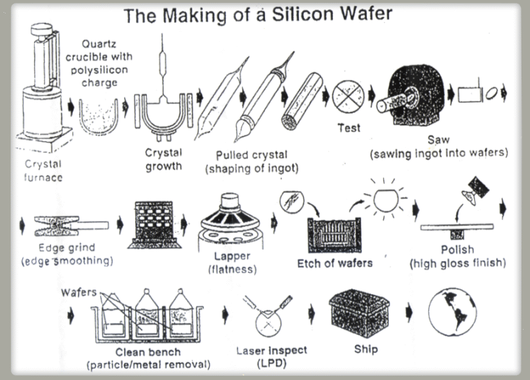
Manufacturing silicon wafers begin
by growing a silicon ingot which can take one week to one month.
More than 75% of all single crystal silicon wafers are grown by
the Czochralski (CZ) method. Ingots are grown by placing chunks
of polycrystalline silicon into a quartz crucible along with small
quantities of dopants. The polycrystalline silicon are made from
sand by means of a complex reduction and purification process
using Trichlorosilane and Hydrogen. The dopants give the desired
electrical properties for the grown ingot and determine the type
of the ingot (P or N).
Crystal Pulling
Polysilicon chunks are loaded into
quartz crucible of the furnace along with small amounts of dopants.
The polysilicon is melted at a process temperature of 1400 deg.
C in a high purity Argon gas ambient. Once the melt is achieved,
a "seed" of a single crystal silicon is lowered into
the melt and slowly pulled out. The surface tension of the seed
and the molten silicon causes a small amount to rise with the
seed, forming a perfect monocrystalline ingot with the same crystal
orientation with the seed.
Shaping
Finished monocrystalline ingot is
ground to a rough size diameter and is either "notched"
or "flatted" along its length to indicate the orientation
of the ingot.
Slicing
Ingots are sliced into wafers using
a diamond ID saw.
Edge grinding
An important step in the manufacturing
of silicon wafer to reduce wafer breakage in the remaining manufacturing
processes or future device manufacturing processes. On Prime wafers,
edges are also highly polished which can improve cleaning results
and reduce breakage up to 400%.
Lapping
Wafers after slicing are rough with
saw marks and defects on both sides of wafers. Lapping removes
saw marks and defects from the surface of the wafers, while also
thins and relieves stress accumulated in the wafer from the slicing
process. In process checks are also conducted during this process
and more fall-out will occur.
Etching and
cleaning
Using sodium hydroxide or acetic
and nitric acids, the microscopic cracks and surface damage caused
by lapping are removed, then followed by deionized water rinses.
Polishing
Polishing requires a number of steps
using progressively finer slurry (polishing compound). Polishing
can be done on frontside or both side of the wafer. Prior to polishing
wafers may receive "backside damag" such as a coating
of polysilicon, bead blast or brush damage. All these treatments
are for the purpose of "Gettering Defects". Gettering
draws defects in the silicon towards the backside of the wafer
and away from the frontside of the wafer where devices are being
built.
Final Cleaning
This step is to remove trace metals,
residues, and particles on the wafers. The cleaning method is
developed by RCA in 1970's. The first part is called SC1 and consist
of Ammonium Hydroxide followed by a diluted Hydrofluoric acid
clean followed by a DI water rinse. Next the SC2 clean consists
of Hydrochloric acid and Hydrogen peroxide followed by DI water
rinse. After this cleaning and rinsing the finished wafers go
through a frontside and backside scrub to remove the smallest
particles.
Final sort
and inspection
Wafers are inspected to meet customer's
specifications. Most final sorting of wafers occurs on an automated
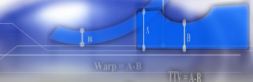
system. These systems measure different parameters such as Thickness,
Bow-Warp, TTV, Site & Global Flatness, Type and Resistivity.
Particles, scratches and haze are measured on a separate automated
system.